Homemade embedded CPU on an FPGA
Part of the series University projects (5 posts total).- May 18, 2023 - My university projects
- May 18, 2023 - RoboCup: Autonomous line following robot competition
- Jun 06, 2023 - Hi-Fi amplifier for record players
- Jun 07, 2023 - Homemade embedded CPU on an FPGA
- Jul 02, 2023 - Rule-Based economic control of HVAC system
On my 4th semester, the theme was digital systems. Someone in our group had a family member with a pellet furnace he would like to design his own controller for, and this somehow evolved into a project in which we created our own CPU on an FPGA. This CPU was then to act as a programmable logic controller (PLC) for a smart home with many devices. At least in theory.

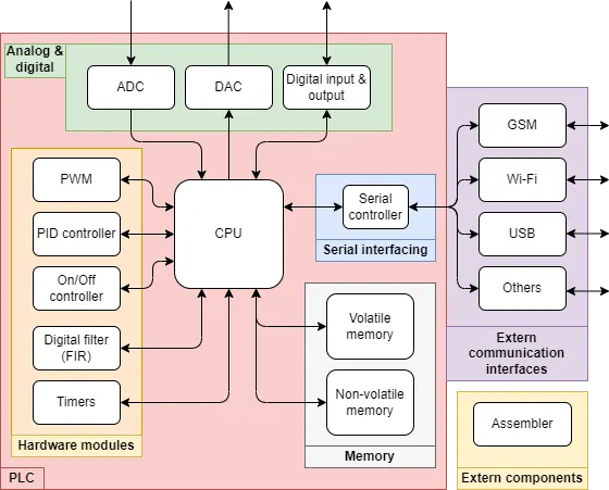
Topology overview of the designed CPU split into several groups.
Due to time constraints we were not able to implement the PID controller and USB interfacing. The CPU is programmed on a field-programmable gate array (FPGA) which is unit consisting of a very large of amount of logic blocks, the connections between which can systematically be programmed using a hardware description language (HDL). In essence, you can program an arbitrary digital circuit (not simulation) by setting the values of multiplexers, look-up tables and charging certain capacitors. This sounds way more difficult than it is, as everything is handled by the FPGA and you just need to specify the circuit in HDL. We use the HDL language VHDL, where the V stands for very high speed (yes this is a real acronym).
The CPU

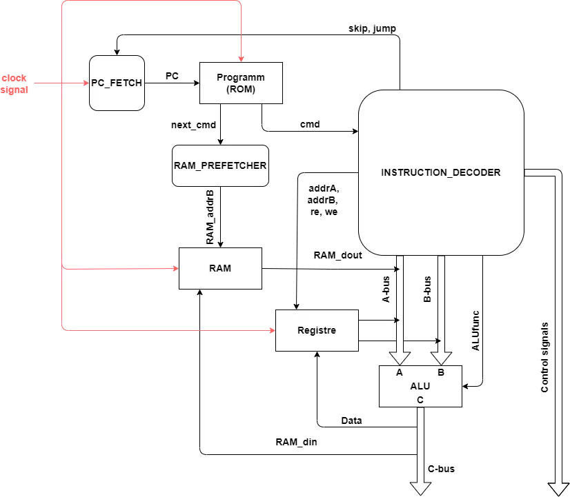
Signal path diagram of the CPU.
CPU structure can be really difficult to follow if you’re outside the know-how. Basically, a CPU runs a program which consists of many lines of instructions. A program counter keeps track of which instruction is next in line. This instruction is decoded and stuff happens. Then the program counter is updated and so on, repeating forever.
If you are a tid bit more nerdy, you can look at the diagram above and the more detailed flow below:
- A rising edge on the clock signal begins a new cycle.
PC_FETCHupdates the program counter (PC) responsible for keeping track of where we are in the code. Normally PC is advanced once forward, but for logic statements (IF, WHILE, ELSE) or jumps the PC must be changed accordingly. This is controlled by theskipandjumpflags set by theINSTRUCTION_DECODER.- The
RAM_PREFETCHERexamines the command for the next PC (if it is known) and begins addressing the memory in preparation for next cycle. It does so by setting the address signal for the RAM block. This is necessary due to the random access memory (RAM) having a read latency of a clock cycle not allowing for fetching and usage of memory in the same cycle. - The
INSTRUCTION_DECODERtakes the current command and performs it. This involves either using the arithmetic logic unit (ALU) or setting various control signals for the hardware modules or extern communication interfaces. - If the
ALUis used, arithmetic between the signal onA-busandB-busis performed. These signals can come from the instruction itself (constants) or from memory (prefetched). TheALUcan perform addition, subtraction, multiplication and logical operations (AND, NOT, OR) only on integers. Floating points (decimal numbers) must be implemented in programming. - The output of the
ALUis placed on theC-buswhere it can go to back into ram, or be connected to some other part of the system depending oncmd. The output of the ALU is also available for the next cycle as it is saved in a register for quick access without RAM usage.
The CPU gets its instructions from RAM. The RAM is split into two ports, one used for storing the program and the other for intermediate variables. The RAM is realized as a true dual port RAM, meaning that each port has their own address signals and outputs and may be accessed concurrently. The instructions are stored and read in machine code which is just a bunch of bits (0’s and 1’s) in memory. Each instruction consists of the operation, called the opcode a register value, called reg and a constant value, called val. The opcode is chosen to be 8 bits, the reg 4 bits and the val 16 bits. An example is seen below, which is the instruction for adding the val of 25 to reg 1.
[OPCODE ]  [REG] [VAL              ]
0000 1110  0001  0000 0000 0001 1001
The reg variable indicates one of 16 16-bit registers which are available to the CPU without latency. These are heavily utilised when programming the CPU as it is much more convenient than RAM at the cost of a small amount of memory.
The assembler
The machine code above is very hard to program and even harder to read. For this reason, we decided that the system must be able to be programmed in another language. The simplest, non-trivial language we could realistically implement in the given time frame was an assembly-like language. An assembly language is a language with very close correspondence to the machine architecture.
Each line consists of an opcode represented by a name possibly followed by a registry and a value just as it is written in machine code. To use constant values the $ (dollar-sign) is used, which transforms the opcode to the corresponding machine instruction for constants.
|
|
Labels are also supported, which allow for the code to branch and jump around and implement logic branches such as IF, WHILE etc.
|
|
The assembler also allows for inclusion of files, such that a program doesn’t have to be written entirely in a single file. The assembler is written in Python and available on GitHub, where you can also find the full list of opcodes.
The hardware modules
As mentioned earlier, the CPU has access to various other modules which function concurrently with the CPU. These are:
- The UART module which is implemented as a first-in first-out (FIFO) buffer with allocated memory and a clock signal down sampled by the CPU to match a specific baud rate.
- An on/off controller with hysteresis where an input, reference and hysteresis limits can be set. It is implemented as a clocked state finite-state machine.
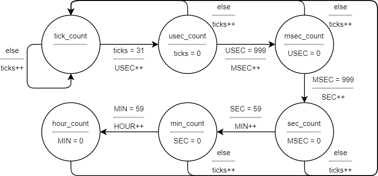
- The timer implemented as a set of registers corresponding to hours, minutes, seconds, milliseconds, microseconds and ticks. These values count up to maximum and roll over into the next register. The timer can be reset, such that all counts go to zero.

Clocked finite-state machine for the timer hardware module.
- The PWM block is implemented as a counter which counts to a variable
COMPAREand outputs 1 as long as the count is above. The count is reset once it hits an arbitraryOVERFLOWvalue. This allows for any duty cycle to be constructed up to the accuracy of the signals, those being 16 bit. - The FIR filter is implemented in direct form as a series of delays, products and multiplications. The internal values of the FIR filter must be decimal compatible, and are done so by fixed-point representation instead of floating points.
The entire project ended up working well, and we made a functional and programmable CPU. At the exam we showcased a test in which we sent a an SMS to the GSM module, which was processed by the CPU which turns a servo motor correspondingly using the UART module. Alongside this, the on/off controller with hysteresis is tested on an LED. A video of the test is seen below.
Conclusion
This was a good introduction to digital systems and in particular to FPGA and VHDL programming. Sadly, this semester was the beginning of COVID-19, so we had to work from home which complicated things. The code for the VHDL implementation can also be found on GitHub but it is sparsely documented.
Published 7. June 2023
Last modified 17. December 2024